It is the purpose of this section to introduce the periodic reliability reports issued by Marktech on our optoelectronic products.
As new products, processes and test procedures evolve, the applicability of past data to reliability changes. Thus, data presented here represents a “snapshot in time” of data believed applicable to the product made now and in the immediate anticipated future.
1. Led lamps and led displays
Reliability Tests:
Reliability Tests are conducted to confirm the design margin and limit levels of devices, or to maintain and confirm the quality assurance levels of mass produced devices.
Though the test methods and test conditions depend on the purpose usually, the electrical stress, thermal stress and mechanical stress during the use of the devices are assumed and their withstand levels are estimated.
Table 3-1 shows the reliability test method of LEDs and led displays.
| Type | Test | Test conditions | MIL-STD-750 Reference |
|---|
| Life | Operating life | Ta = 25°C IF Max. rating | 1026.3 |
| Life | High temperature storage | Ta = Tstg., Max. | 1026.3 |
| Life | Low temperature storage | Ta = Tstg., Min. | – |
| Life | High temperature and high humidity storage | Ta = 60°C or 40°C, R. H. = 90° | – |
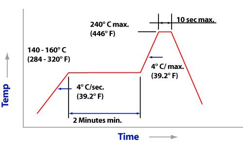
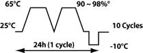
| Enviromental | | Immersed for 10 sec. at 260° up to 2mm from the body | 2031.1 |
| Enviromental | | Tstg. Min. ~25°C~ Tstg. Max. ~25°C (30 min.) (5 min.) (30 min.) (5 min.) | 1051.1 |
| Enviromental | | 100°C or Tstg. Max. ~0°C 3 sec. transfer in water | 1051.1 |
| Enviromental | Moisture resistance | | 1021.1 |
| Enviromental | | 100~2000~100 Hz 4 cycles each X, Y, Z at 20G | 2056 |
| Enviromental | | 3 blows, 1500G, 0.5 (lamps)
3 blows, 500G, 1 ms (displays) | 2006 |
| Enviromental | | 1 minute each X, Y, Z at 20,000 (lamps)
1 minute each X, Y, Z at 5000G (displays) | 2006 |
| Enviromental | | Weight 250 g, 0° ~ 90° ~0° bend, 3 times | 2036.3 |
| Enviromental | | Immersed for 5 sec. at 230°C flux: 75% isopropyl alcohol, 25% WW resin | 2026.2 |
Reliability test methods – life tests
| Measuring terms | Failure criteria |
|---|
| Luminous Intensity(IV) | Lower standard limit X 0.5 |
| Forward voltage(VF) | Upper standard limit X 1.2 |
| Reverse leakage current (IR) | Upper |
Operating Life Test: To confirm the stability during usual operation, the maximum rating forward current at room temperature is applied to the LEDs.
Storage Life Test: To confirm the stability in storage, the high and low temperature storage life tests are conducted under the conditions of the maximum and minimum storage temperature. Since the devices may be used or in storage at high temperature and high humidity, therefore the high temperature and high humidity storage life test is conducted.
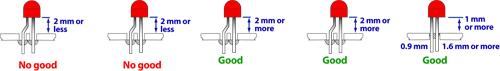
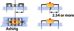
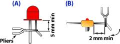
Environmental Test: Since the estimation of thermal stress and mechanical stress applies to the rating, the attaching and using of the devices, the soldering heat, temperature cycles, thermal shock, vibration and lead strength etc. are examined.
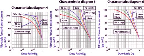
*PW = 100μs, DR = 10-1
Reliability test data – The measuring terms and failure criteria are as follows:
Prediction of Failure Rate
Based upon field experience and our extensive test data, the failure mode when using LEDs are dominated by accidental failures (open, short, etc.) rather than the degradation of the luminous intensity. These accidental failures are considered to result from, carelessness in the manufacturing process; fatigue due to the thermal stress and mechanical stress etc.; breakdown due to over voltage (current). Accordingly if we take into account these accidental failures, the failure rate can be predicted.
From our field experience and our extensive test data, this accidental failure rate can be estimated to be about 10 to 50 Fit.
Regarding the luminous intensity (IV) which is the main characteristic of LEDs, the half-life (time when the luminous intensity has been reduced to 50% of the initial value) obtained from the accelerated operating life test, is estimated as shown in Figure 3-2.
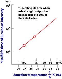
Figure 3-2 – Junction temperature